
Photolithography: printing circuits onto silicon
The smallest features on a modern chip are a few nanometres across, smaller than most viruses. They are not carved but printed with light. This covers the four-step cycle, the Rayleigh criterion, the multi-patterning era, and why EUV is so hard.
A modern processor holds tens of billions of transistors, with the smallest features a few nanometres across — smaller than most viruses. These are not carved; they are printed with light. You coat a silicon wafer with a photosensitive resist, block the light with a mask, let the light draw a pattern in the resist, then transfer that pattern into the silicon.
The process is called photolithography, and it is the one step in semiconductor manufacturing that decides how small anything can get.
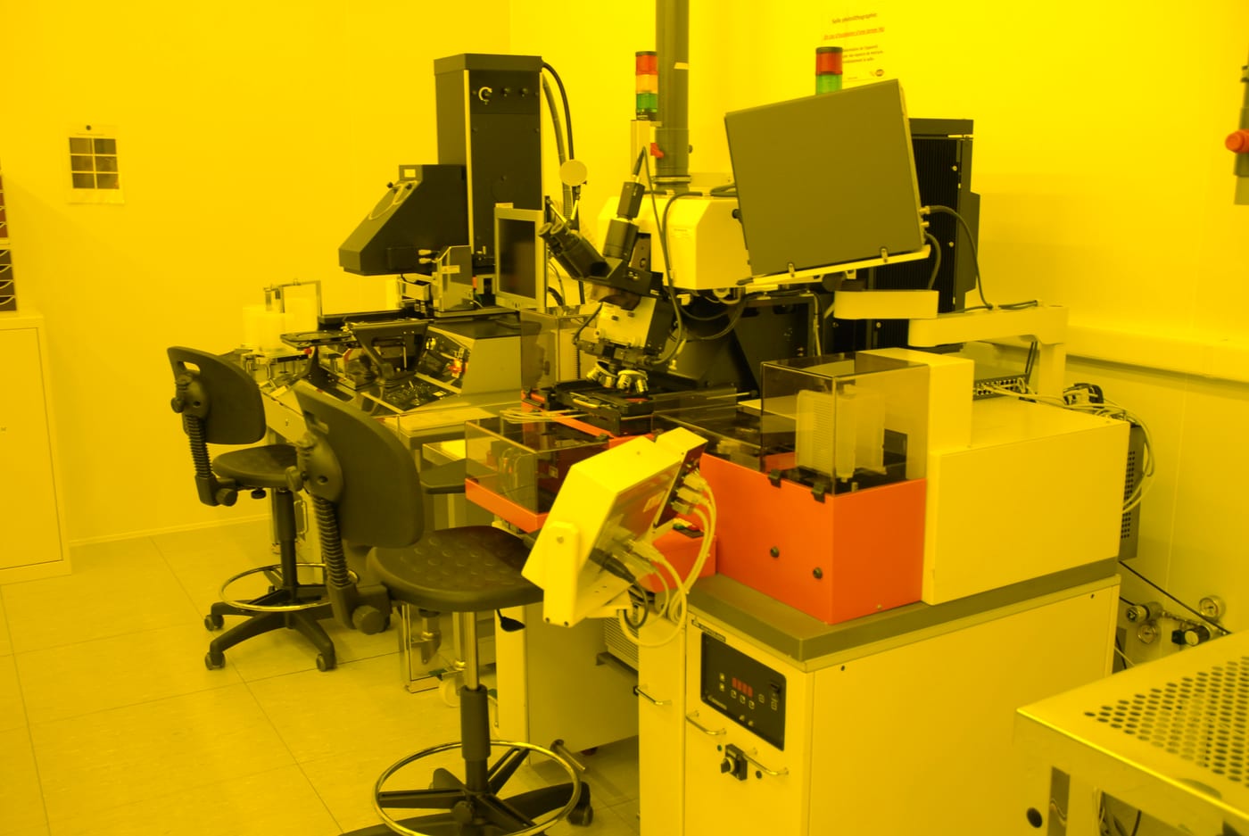
Image: Guillaume Paumier, CC BY-SA 3.0, via Wikimedia Commons.
Four steps, one cycle
One lithography cycle looks roughly like this:
- Coat: spin photoresist into a uniform film tens to hundreds of nanometres thick. In a positive resist the exposed area becomes soluble; a negative resist is the opposite.
- Expose: light passes through the mask and is demagnified 4x by the projection lens onto the resist. This step fixes the shape and position of the pattern.
- Develop: a developer dissolves the exposed (or unexposed) resist, leaving the pattern behind.
- Etch or deposit: using the remaining resist as a mask, cut the pattern into silicon, oxide or metal — or grow a layer on top.
Then strip the resist and repeat. An advanced logic chip has sixty to a hundred such layers, each needing its own mask set.
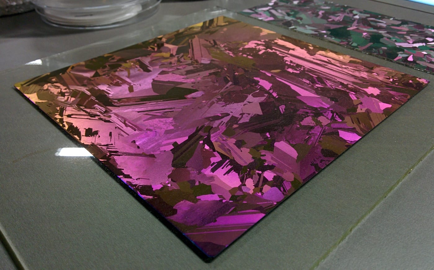
Image: Radiotrefoil, CC BY-SA 4.0, via Wikimedia Commons.
How small you can go, in one formula
The resolution limit is approximated by the Rayleigh criterion:
CD = k1 × λ / NAEach term has its own lever:
| Term | Meaning | How it shrinks |
|---|---|---|
| λ | wavelength of the light | 436 nm mercury lamp → 193 nm ArF excimer laser → 13.5 nm EUV |
| NA | numerical aperture of the lens | 0.93 dry → 1.35 immersion (water between lens and wafer) |
| k1 | process factor | pushed down by resolution enhancement; theoretical floor 0.25 |
Wavelength went from 436 nm to 13.5 nm, a factor of thirty. This is not a better light bulb: every change of wavelength means rebuilding the optics, the resist chemistry and the mask materials.
The 193 nm wall, held back by multi-patterning
Pair 193 nm light with an immersion lens and NA reaches 1.35, which in theory resolves around 40 nm in one shot. Advanced nodes want a few nanometres. That gap was bridged by multi-patterning for well over a decade.
The idea: if one exposure cannot resolve two closely spaced lines, print one line, chemically deposit sidewalls on both sides of it, then use those sidewalls as a mask to etch two lines — doubling density. That is SADP; a second round gives SAQP, quadrupling it. The cost is more process steps, more expense and more defects.
The other route is computational lithography. Light diffracts through the mask, so a square drawn on the mask lands as a rounded shape on the wafer. So invert the problem: simulate the distortion and draw the mask as a distorted shape with assorted tiny assist features, so that after diffraction it becomes exactly the desired pattern. A modern mask is unreadable to the human eye.
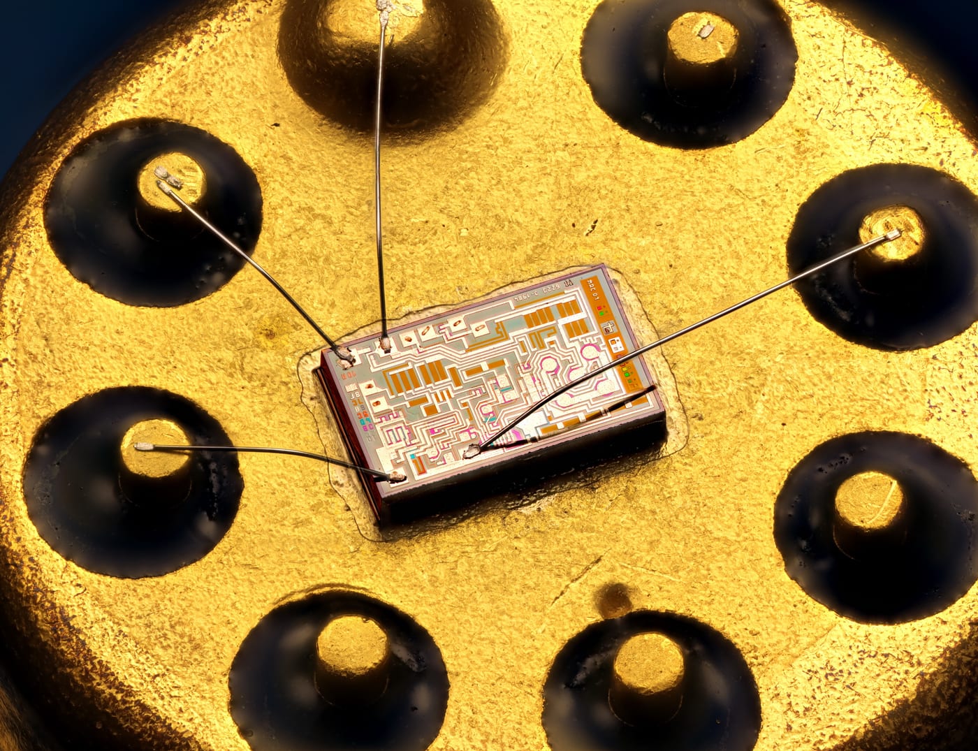
Image: Mister rf, CC BY-SA 4.0, via Wikimedia Commons.
Why EUV is so hard
Extreme ultraviolet lithography uses 13.5 nm light. That number was not chosen — it is the wavelength at which a molybdenum/silicon multilayer reflects best. There is no alternative.
13.5 nm light is absorbed by almost everything, including air. Therefore:
- the entire optical path must be in vacuum;
- lenses are impossible (they absorb), so only multilayer mirrors work, each made of roughly fifty alternating molybdenum/silicon pairs;
- each mirror reflects about 70%; after a dozen mirrors in the path, only a few percent of the energy reaches the wafer;
- the source is a tin droplet: droplets about 25 micrometres across, tens of thousands per second, each flattened and then blasted by a high-power CO2 laser to form a plasma that radiates at 13.5 nm.
The complexity of the whole system leaves exactly one company able to ship a complete machine, with its mirrors coming from another small firm that does nothing but optics. That is not monopoly so much as a division of labour so deep that only a handful of players can stand in it.
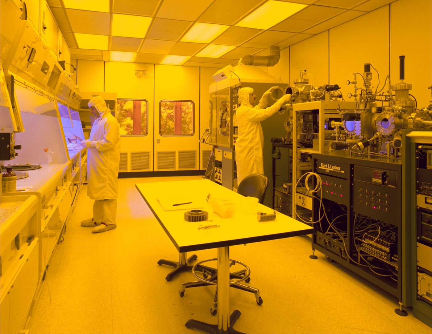
Image: public domain, via Wikimedia Commons.
My take
The counter-intuitive thing about lithography is that there is no next breakthrough to wait for.
Getting from 436 nm to 193 nm took twenty years; from 193 nm to 13.5 nm took nearly twenty more. And the next visible stop after EUV — High-NA, raising NA from 0.33 to 0.55 — is the same physics with bigger, more expensive, harder-to-build mirrors.
So real progress increasingly comes from somewhere else: advanced packaging that stitches multiple dies together, 3D stacking that piles up memory, architectures that bake in dedicated units. Moore’s law is not dead; it is simply being carried by five different directions at once, and lithography is only one of them — the hardest one.
Comments
…